Difference between revisions of "PCB Printer"
Jwhipple15 (talk | contribs) (Created page with "{{#set: |Is equipment=True |Is located in facility=PCB Lab |Is located in facility=The Hub |Is used in domain=Electronics |Has function=Soldering Iron |Has icon=File:sol...") |
|||
| (279 intermediate revisions by 14 users not shown) | |||
| Line 2: | Line 2: | ||
|Is equipment=True | |Is equipment=True | ||
|Is located in facility=PCB Lab | |Is located in facility=PCB Lab | ||
| − | |||
|Is used in domain=Electronics | |Is used in domain=Electronics | ||
| − | |Has | + | |Has name={{PAGENAME}} |
| − | |Has icon=File: | + | |Has icon=File:PCB_printer_icon.png |
| − | |Has icondesc= | + | |Has icondesc=Voltera Icon |
| − | |Has image=File: | + | |Has iconwname=File:PCB_printer_icon_name.png |
| − | |Has imagedesc= | + | |Has image=File:voltera-vone.png |
| − | |Has description= | + | |Has imagedesc=The Voltera V-One PCB Printer |
| − | |Has certification=https:// | + | |Has description= |
| − | + | |Has certification=https://georgefox.instructure.com/courses/1288 | |
| − | + | |Has model=V-One | |
| − | + | |Has group=Circuit Board Design | |
| − | + | |Has make=Voltera | |
| − | + | |Has serial number=V1-05-0129-120 / V1-04-0183-120 | |
| − | + | |Has ace=Nick Scianna;nscianna18@georgefox.edu | |
| − | |||
| − | |||
| − | |||
}} | }} | ||
| + | [[{{#show: {{FULLPAGENAME}}|?Has icon|link=none}}|140px|left|{{#show: {{FULLPAGENAME}}|?Has icondesc}}]] | ||
| + | [[{{#show: {{FULLPAGENAME}}|?Has image|link=none}}|300px|thumb|upright=1.5|{{#show: {{FULLPAGENAME}}|?Has imagedesc}}]]Make: {{#show: {{PAGENAME}} |?Has make}} | ||
| − | + | Model: {{#show: {{PAGENAME}} |?Has model}} | |
| − | |||
| − | + | Serial Number: {{#show: {{PAGENAME}} |?Has serial number}} | |
| − | |||
| − | + | Ace: {{#show: {{PAGENAME}} |?Has ace.Has name}} ({{#show: {{PAGENAME}} |?Has ace.Has email address}}). | |
| − | + | Location: {{#show: {{PAGENAME}} |?Is located in facility}} | |
| − | |||
| − | |||
| − | |||
| − | |||
| − | |||
| − | + | __TOC__ | |
| − | === | + | ==Description== |
| − | |||
| − | |||
| − | |||
| − | |||
| − | |||
| − | |||
| − | |||
| − | + | The PCB Printer (Voltera V-One) brings quick turn PCBs to your desktop. Import your Gerber file into the Voltera software, press print, and the V-One will bring your board to life. Use the drilling, solder paste dispensing, and reflow features to mount components onto your printed board, or mount components on a pre-fabricated board with ease. | |
| − | + | This is a simple example of what the PCB Printer can do. Currently the PCB lab has a different baking process using a different oven, so we will be curing the boards using a different method than shown in the video. | |
| − | = | + | {{#evu:https://www.youtube.com/watch?v=N6nEgN4THRE}} |
| − | + | ==Documentation== | |
| − | |||
| − | |||
| − | |||
| − | |||
| − | |||
| − | |||
| − | |||
| − | |||
| − | |||
| − | |||
| − | |||
| − | |||
| − | |||
| − | |||
| − | |||
| − | |||
| − | |||
| − | |||
| − | |||
| − | |||
| − | + | ====Terminology==== | |
| − | + | The following conductive inks and pastes are stocked in the PCB Lab. Each material requires a special heating program setting. See each individual material below for the proper reflow oven setting. | |
| − | + | Inks are also identified by a lot name and expiration date. If properly installed, the expiration date should be viewable through the window in the dispenser, but the lot name will not. Refer to the label on the back of the dispenser for the lot name. When selecting the ink you're using in the Voltera software, it will identify the ink by type, lot name, and expiration date. Make sure you select the correct one. | |
| − | + | [[File:voltera_aqueous.PNG|frameless|left|200px]] | |
| − | + | '''Conductive Ink''' | |
| − | |||
| − | |||
| − | |||
| − | |||
| − | |||
| − | + | - Use to lay conductive traces on substrates (Green is "V1 Ink" setting on Reflow Oven) | |
| + | <br /><br /><br /> | ||
| − | + | [[File:voltera_furious.PNG|frameless|left|200px]] | |
| + | '''Solder Paste''' | ||
| − | + | - Use only on boards that utilize Voltera's ink traces, such as the ink above. (Orange is "V1 Paste" setting on Reflow Oven) | |
| + | <br /><br /><br /> | ||
| − | + | [[File:voltera_armored.PNG|frameless|left|200px]] | |
| + | '''Solder Paste Sn63 Pb37''' | ||
| − | + | - Use only premade boards, such as ones from [https://jlcpcb.com/ JLCPCB] (Blue is "Sn63Pb37" on Reflow Oven) | |
| − | |||
| − | + | <br /> | |
| + | <br /> | ||
| − | + | <gallery> | |
| + | File:Voltera substrates.jpg|Substrates | ||
| + | File:Vone probe.jpg|Probe | ||
| + | File:Dispenser and Sheath.jpg|Dispenser and Sheath | ||
| + | File:Voltera conductive ink.png|Conductive Ink Cartridge | ||
| + | File:Voltera 225 nozzle.jpg|Nozzle - 225 Micron | ||
| + | File:Voltera burnish.jpg|Burnishing Pads | ||
| + | </gallery> | ||
| − | + | [[Media:Voltera_V-One_Manual_English.pdf|Voltera User Manual]] | |
| − | + | [https://support.voltera.io/circuit-design-guidelines Circuit Design Guidelines] | |
| − | |||
| − | |||
| − | |||
| − | + | [https://support.voltera.io/altium#main Altium Gerber Export Guide] | |
| − | |||
| − | + | [https://www.voltera.io/ Voltera Home Page] | |
| − | + | [https://support.voltera.io/hc/en-us/sections/115001325748-User-Guides User Guides] | |
| − | |||
| − | |||
| − | + | ==Before you Print== | |
| − | |||
| − | |||
| − | |||
| − | + | Here are a few things to check before exporting your gerber files and fabricating your PCB. [[File:Voltera-drillbits.png|thumb|300x300px|right|Available drill bit sizes]] | |
| − | |||
| − | |||
| − | |||
| − | + | #Verify via hole sizes. | |
| − | + | ##Based on the size of what needs to go in the via, select a rivet with the proper internal diameter from the table on the [[Through Hole Press]] page. | |
| + | ##Once you've selected the rivet size, take the outer diameter of the rivet from the table and add 0.1mm. | ||
| + | ##Check this outer diameter against the available drill sizes for the Voltera (see the image to the right). Round up to the nearest drill size and use that for the hole size in Altium. | ||
| + | #Verify annular ring size | ||
| + | ##Your annular rings (via diameter) should be at least as large as the head diameter of the rivets you plan to use, otherwise they might not make good contact. | ||
| + | #Check that your design follows the circuit design guidelines at the link above | ||
| − | ===== | + | ==Training== |
| − | + | ====Operation==== | |
| − | + | The PCB Printer is a fantastic tool for prototyping PCBs. After uploading Gerber files from Altium or a related software, the Voltera will be able to print traces and pads. The Voltera has the ability to bake traces and reflow components on its heated bed, but you will need to use the reflow oven to bake boards. The PCB Lab uses the reflow oven for baking due to the amount of people it needs to accommodate, so users will only be using the PCB Printer to print traces and pads. The Conductive Ink (used for Traces) is indicated by a green dot on the dispenser, the Voltera Solder Paste (used for Pads) is indicated by an orange dot on the dispenser, and the Manufactured Solder Paste (used for Pads) is indicated by a blue dot on the dispenser. | |
| − | |||
| − | |||
| − | |||
| − | |||
| − | |||
| − | |||
| + | Before beginning with your PCB, it is imperative that it is completely flat, meaning no components are installed, as it will result in breaking the nozzle of the dispenser, or it will be unable to calibrate correctly. | ||
| − | + | ====Demonstration==== | |
| − | + | To show a complete knowledge of the PCB Printer, the student will design a PCB in Altium or related software, print the traces/pads, and transition to the Reflow Oven. As a part of the process, the student will also perform correct set up and shut down procedures, all of which can be found in the General Procedure below. | |
| − | ==== | + | ====General Procedure==== |
| − | |||
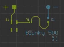
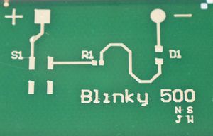
| − | + | Using the Voltera to create single-sided boards with NO vias or holes.[[File:voltera_blinky_500.jpg|300x300px|thumb|right|Training board - The Blinky 500]] | |
| − | + | #'''Drilling''' | |
| + | ##'''This board in particular does not have any holes, so this entire step can be skipped for this procedure''', however, these are the steps to take if you need to drill holes in the future. | ||
| + | ##After opening the Voltera software, select Drill. This option is chosen only if you want to add holes to an existing board. | ||
| + | ##For Drilling, you can either choose the Simple or Aligned route. Choose Simple if your board has no existing features, and choose Aligned if your board has some existing features. Lets go through the process for both. | ||
| + | ##Drilling for a Simple Board | ||
| + | ###Alrighty, you've chosen Simple, so this procedure assumes there is absolutely nothing fabricated on the board. Not gonna lie, this procedure is a little more sketchy than aligned simply because you literally eyeball your board's outline. The no eloquent calibration system. That's just how it works. | ||
| + | ###Voltera will ask you to upload your Ink and Hole files. Remember, the correct Hole file will say Plated in the name. This will allow you to calibrate the Voltera later and it supplies the drill locations. | ||
| + | ###Then it will ask you to move your boards location on the plate so the Voltera knows where it needs to drill. This is the sketchy part. It outlines a square, and you make a judgement based on what it thinks. If it outlines too low, move your circuit up further on the plate to compensate for it. If it outlines too far to the left, move your circuit to the right on the plate to compensate for it. Continue this process until it looks "good enough." | ||
| + | ###Use the clamps and screws to secure your board. It would be such a shame if it moved during fabrication... [[File:Board.jpg|none|thumb|300x300px]] | ||
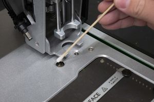
| + | ###Mount the probe on machine. This will help us calibrate the machine. It will move to the wrong spot initially, but then it is your duty to move the probe into the correct spot. Lowering the probe will allow you to make fine tune movements to optimize the alignment.[[File:Voltera mount_probe.jpg|none|300x300px|thumb]] | ||
| + | ###Once the alignment is complete, it will measure the height of every part of the board. It will take a couple minutes, so just be patient. The transition between printing and drilling is done with the same alignment. | ||
| + | ###Once that is complete, it is time to select the holes we want to drill. '''All the holes you select are highlighted in Green.''' Remove the probe and select which holes you want to drill. Remember not to drill the holes that already exist![[File:...holes.png|none|thumb|300x300px]] | ||
| + | ###Select the corresponding drill bit, put it into the drill, mount it, and plug it in. Be extra careful not to break anything. People usually break it because while they are mounting it, the drill hits the Voltera and snaps. It's okay to push it into the drill pretty far, and this will keep you from breaking it. '''DON'T FORGET TO USE THE ALLEN WRENCH TO SECURE THE BIT!''' | ||
| + | ###The drill should sing you a little song once it's connected. '''Before drilling, prepare the vacuum.''' Use this to suck all the debris that comes from your board. You can get it decently close to the board, even on the board while it is drilling, just be sure to move when the drill is getting ready to move.[[File:VacuumBoi.jpg|none|thumb]] | ||
| + | ###And you're finished drilling holes! Vacuum up any debris and continue with laying the traces. | ||
| + | ##Drilling for an Aligned Board | ||
| + | ###Awesome, you've chosen Aligned, so this procedure assumes you have some preexisting holes and the like on the board. | ||
| + | ###Voltera will ask you to upload your Ink and Hole files. Remember, the correct Hole file will say Plated in the name. This will allow you to calibrate the Voltera later and it supplies the drill locations. | ||
| + | ###Use the clamps and screws to secure your board. It would be such a shame if it moved during fabrication...[[File:Board.jpg|none|thumb|300x300px]] | ||
| + | ###Mount the probe on machine. This will help us calibrate the machine. It will move to the wrong spot initially, but then it is your duty to move the probe into the correct spot. Lowering the probe will allow you to make fine tune movements to optimize the alignment.[[File:Voltera mount_probe.jpg|none|300x300px|thumb]] | ||
| + | ###Once the alignment is complete, it will measure the height of every part of the board. It will take a couple minutes, so just be patient. | ||
| + | ###Once that is complete, it is time to select the holes we want to drill. '''All the holes you select are highlighted in Green. Anything that is highlighted in Green will be executed.''' Remove the probe and select which holes you want to drill. Remember not to drill the holes that already exist![[File:...holes.png|none|thumb|300x300px]] | ||
| + | ###Select the corresponding drill bit, put it into the drill, mount it, and plug it in. Be extra careful not to break anything. People usually break it because while they are mounting it, the drill hits the Voltera and snaps. It's okay to push it into the drill pretty far, and this will keep you from breaking it. '''DON'T FORGET TO USE THE ALLEN WRENCH TO SECURE THE BIT!''' | ||
| + | ###The drill should sing you a little song once it's connected. '''Before drilling, prepare the vacuum.''' Use this to suck all the debris that comes from your board. You can get it decently close to the board, even on the board while it is drilling, just be sure to move when the drill is getting ready to move.[[File:VacuumBoi.jpg|none|thumb]] | ||
| + | ###And you're finished drilling holes! Vacuum up any debris and continue with laying the traces. | ||
| + | #'''Ready the Ink''' | ||
| + | ##The ink is most usable when it reaches room temperature, so we have to let it warm up in advance. | ||
| + | ##Grab the correct conductive ink from the fridge, and let it warm up to room temperature, about 15-30 minutes. It is labeled with a '''green''' sticker. | ||
| + | #'''Software Setup''' | ||
| + | ##Download the files for this project [[Media:Pcb printer level 1.zip|here]]. | ||
| + | ##Power on the Voltera. | ||
| + | ##Open the Voltera Windows application. | ||
| + | ##Select "Print" and then "Simple." "Print" indicates that we want to print traces, and "Simple" indicates that the board is not pre-fabricated. If we had a pre-fabricated board, we would instead select "Aligned" so we can align the holes. | ||
| + | ##Next we need to add the proper conductive ink, which is the same conductive ink you acquired in step 1.2. | ||
| + | ##Load the ink file from the project files. This is the Top Layer Gerber file. | ||
| + | #'''Clamping the Substrate''' | ||
| + | ##Acquire a 1.5" by 2" blank board. They are located in the one of the drawers. | ||
| + | ##Slide the board underneath the clamps on the Voltera, push the clamps towards each other, and finger-tighten the thumb screws. You should not be able to move the board once you clamp them down. [[File:Voltera clamping.jpg|border|none|300x300px]] | ||
| + | #'''Mounting the Probe''' | ||
| + | ##Pull the probe from one of the drawers. The probe should have a large metal tip, do not confuse it with the dispenser. [[File:Voltera drawer.jpg|border|none|300x300px]] | ||
| + | ##Remove the cap and place it near the Voltera. | ||
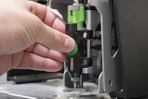
| + | ##Mount the probe onto the magnetic gantry. It should snap into place and the contacts should align. [[File:Voltera mount_probe.jpg|border|none|300x300px]] | ||
| + | #'''Positioning and Probing''' | ||
| + | ##Click "Outline." This will show you where the Voltera thinks the board is. It will move the probe around the printer surface and determine how close the dispenser will need to be to the board. | ||
| + | ##Repeat step one until the outline is centered with the board. Click and drag the circuit in the Voltera application to move the outline. | ||
| + | ##'''You MUST ensure the outline does not collide with the clamps AND does not exceed the dimensions of the board!''' Do NOT proceed until this is checked! | ||
| + | ##In the next step, Click "Probe" and wait for the Voltera to finish its measurements. [[File:Voltera probing.jpg|border|none|300x300px]] | ||
| + | ##Remove the probe, replace the cap, place the probe back in the drawer, and proceed. <br /><br /> | ||
| + | #'''Priming the Conductor''' | ||
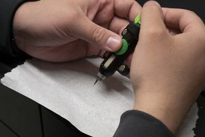
| + | ##Ensure 15 minutes have passed before beginning the next step. This helps the ink flow easier, so the dispenser should not be cold to the touch. | ||
| + | ##'''Read carefully.''' The Voltera application explains this step well. Follow the on-screen instructions before moving on to the next step. Some tips/tricks/warnings:<br /> - '''Nozzles are fragile!''' You would be surprised how easy it is to break one. Treat this process with care!<br /> - Hold the dispenser over a paper towel to prevent ink from getting everywhere.<br /> - If you need to wipe the nozzle, do so '''gently''' and '''use a cotton swab found in the drawers.''' <br /> - Ink should not be flowing quickly out of the dispenser when you finish priming, but '''a very small amount''' of flow is OK. <br /> [[File:Voltera priming.jpg|border|none|300x300px]] | ||
| + | ##Mount the dispenser. [[File:Voltera mount_conductive.jpg|border|none|300x300px]] | ||
| + | #'''Calibration''' | ||
| + | ##Click "Advanced." Start with the '''Z at 0.10 mm''' and the '''E at 0 um'''. Adjust the Voltera to these values, as it is a safe distance for the dispenser. | ||
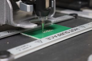
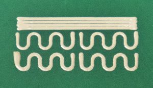
| + | ##Click "Calibrate." The Voltera will lay down a test print. Pay close attention to the amount and consistency of the ink.[[File:Voltera calibrate.jpg|border|none|300x300px]] | ||
| + | ##The example below has slightly too much ink. Notice how a portion of the horizontal lines touch and some parts of the ink glob up. [[File:Voltera calibrate_bad.jpg|border|none|300x300px]] | ||
| + | ##In this case, to make an adjustment, the ink height was set to a '''Z of 0.09 mm''' and the flow was set to an '''E of -10 um.''' This dispenses less ink than before. | ||
| + | ##'''You may need to do the same or make different adjustments. Whatever you do, do NOT run the nozzle into the board! The nozzle will break!''' | ||
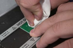
| + | ##If an adjustment was made, '''wipe the board clean with a paper towel (shown below) and/or clean it with isopropyl alcohol''' and repeat the calibration. [[File:Voltera calibrate_wipe.jpg|border|none|300x300px]] | ||
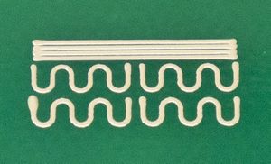
| + | ##The example below is a more acceptable test print. Strive for this consistency. If your board looks right, proceed. [[File:Voltera calibrate_better.jpg|border|none|300x300px]] | ||
| + | ##Click "Next," and wipe the board clean a final time, as you are now preparing to print your whole circuit. <br /><br /> | ||
| + | #'''Top Layer Print''' | ||
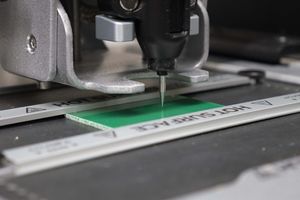
| + | ##'''The Voltera will print what is selected in Green.''' Below is an example of a portion of the board selected. Ensure the portion you want to print is selected (in this case, select everything.) '''Remember that blue lines will not be printed.''' [[File:voltera_selection.PNG|300x300px|none]] | ||
| + | ##Click "Start." Let the Voltera finish its process. If a portion of the print fails or is incorrect, you can stop mid-print, or wait until it is finished and redo that selection. Also shown below is an example of a portion of ink that globbed up. The portion was wiped and can be reprinted. [[File:voltera_printing.jpg|300x300px|none]] <br /> [[File:voltera_print_blob.jpg|300x300px|none]] <br /> [[File:voltera_print_redo.jpg|300x300px|none]] <br /> | ||
| + | ##Remove the conductive ink, put the cap back on, '''and return the conductive ink to the fridge!''' | ||
| + | ##When you reach the instruction titled "Flip Board," you are done. We want to bake these traces on the Reflow Oven before we do anything else to the board. | ||
| + | ##Unclamp the board from the Voltera, and remember that the traces are still wet, so do not smear them around. | ||
| + | ##Consult the Reflow Oven wiki and complete that process. Bake the board soon after printing to ensure best results. | ||
| + | #'''Preparing for Solder Paste''' | ||
| + | ##You should now have a PCB with traces baked on it! Time to make those pads for placing components. | ||
| + | ##Take a burnishing pad from one of the drawers. Rub the substrate with the pad until the traces have a shine to them, rather than a dull appearance. | ||
| + | ##Replace the burnishing pad back into the drawer. This cleans the surface of the traces and makes them look super shiny. | ||
| + | #'''Aligning the Paste''' | ||
| + | ##This process will help the Voltera know where it needs to print solder. The user gives it two locations where the pads should go, and the Voltera can use the Gerber files to determine where else pads need to go. | ||
| + | ##At this time, retrieve the solder paste from the fridge and set it out to warm. The correct paste is labeled with an '''orange''' sticker. | ||
| + | ##Take the board back to the Voltera and clamp the board into place. Again, you should not be able to move the board after it is clamped. | ||
| + | ##Open the Voltera application and choose "Solder," and choose the proper paste. In this case you want the '''orange'''-labeled paste. | ||
| + | ##Clean the calibration switches, mount the probe, and proceed. | ||
| + | ##Click 'Move to feature." This will move the probe to a pre-determined feature and should not be aligned properly on the first go. It is your job to align it correctly. | ||
| + | ##First, use the arrow keys to roughly align the feature with the probe. This process will help the Voltera know where it needs to put the pads. | ||
| + | ##Next, click "Lower," and use the arrow keys to fine-tune the alignment. Your precision in these steps is key to getting solder paste in the correct places. | ||
| + | ##Click "Measure" when the alignment is correct. The board will be probed and the head will move to a second feature. | ||
| + | ##Repeat steps 8 and 9. | ||
| + | ##Click "Measure." The alignment is now finished. | ||
| + | ##You can confirm the alignment by clicking various features and seeing if the head moves to the right position. If something is off, you can go back and realign if necessary. Proceed until you need to measure the height of the board. | ||
| + | ##Click "Probe." This will measure the height of the board and determine how far away the dispenser needs to be from the board. | ||
| + | ##Once it finishes probing, remove the probe and replace it in the drawer. | ||
| + | #'''Priming the Paste''' | ||
| + | ##Refer to the priming directions in step 8 before mounting the dispenser. | ||
| + | ##Once it is primed, mount it and proceed. | ||
| + | ##Click "Dispense." The paste will dispense onto all of the selected pads. | ||
| + | ##Strive for good coverage of paste, preferably covering most of the pad, if not all of it. | ||
| + | ##Remove the dispenser. Twist the knob clockwise to back off the paste. '''Put it back in the fridge,''' and quit the Voltera app. | ||
| + | ##Unclamp the board from the Voltera. Remember that you are handling a board with wet paste. Clean up! | ||
| + | #'''Cleaning up''' | ||
| + | ##Clean any leftover paste or ink from the calibration switches by rubbing them with a dry cue tip before it dries. | ||
| + | ##If any ink or paste remains elsewhere on the machine, use a cue tip or kimwipe with a little bit of isopropyl alcohol to clean it. Be careful not to drench the machine in isopropyl, as it could let gunk get into the machine and jam things up. [[File:Voltera cleaning.jpg|border|none|300x300px|Cleaning the calibration switches]] | ||
| − | + | You are now done with the PCB Printer! Refer to the Pick and Place as well as the Reflow Oven wikis for the remainder of the process. | |
| − | |||
| − | ==== | + | ==Safety== |
| − | |||
| − | + | #When the PCB Printer is moving and doing its thing, just let it be. Interfering will result in breaking equipment and possibly hurting yourself, especially with the drill. Voltera gives excellent advice/steps for their PCB fabrication process, be sure to follow them. | |
| + | #If you feel like you do not know what you are doing, ask someone for help. You could damage both the equipment and possibly hurt yourself. Do not hesitate to ask or confirm at any point during the process. | ||
| − | + | ==Certification== | |
| − | + | ||
| − | + | [https://georgefox.instructure.com/courses/1291 Canvas Quiz] | |
| − | + | ||
| − | + | ==Troubleshooting== | |
| − | + | ||
| − | + | #Drilling | |
| − | + | ##If your holes seem to be all out of wack, be sure to confirm the following: you should be using the vacuum to suck up any debris that comes from drilling your board while it is drilling. The pieces can interfere with your part. | |
| − | + | ##If they seem to be drilling in the wrong places, then it probably isn't aligned correctly. Go back in the process and start over. | |
| − | + | #Calibration/Alignment | |
| + | ##During the probing process, be sure that your board is completely flat and that the clamps cover a minimal amount of the board while keeping it secure. If the probing hits the claps or runs off the board, the calibration is no good. Go back to the initial stages where you align holes/indicate where to print traces. | ||
| + | ##When holes are available during the Alignment stage, always use them to align your board. NEVER use pads or traces unless you absolutely have to. Holes are much easier to align with. | ||
| + | #Printing Traces/Solder | ||
| + | ##Be sure that the dispenser has been warming up to room temperature for at least 15 minutes so the ink can flow smoothly. | ||
| + | ##If the ink does not seem come come out even when you're priming the dispenser, chances are that it is clogged. Remove the tip, notify a PCB Lab worker, and install a new tip (ask a worker if you don't know how). | ||
| − | ==== | + | ==Maintenance== |
| − | + | ====General maintenance==== | |
| + | The PCB Printer has a few items that need to be maintained by the student or the Ace. Refer to the table below to see each procedure, how often it should occur, and the the last completion of the specific task. | ||
| − | + | ====Specific Maintenance Tasks==== | |
| − | ==== | + | {| class="wikitable" |
| − | + | !Maintenance Procedure | |
| − | -- | + | !Frequency |
| + | !Done By | ||
| + | !Last Completion | ||
| + | |- | ||
| + | |General Cleaning | ||
| + | |Before and after each use, including ink/solder residue and drilled material | ||
| + | |Student | ||
| + | |N/A | ||
| + | |- | ||
| + | |Refrigerating the Dispensers | ||
| + | |Whenever they are not in use | ||
| + | |Student | ||
| + | |N/A | ||
| + | |- | ||
| + | |Replacing Sacrificial Layer | ||
| + | |When the existing layer is worn through and can potential damage the heating bed | ||
| + | |Ace | ||
| + | | | ||
| + | |- | ||
| + | |Replacing Nozzle | ||
| + | |When the nozzle is clogged | ||
| + | |Student or Ace | ||
| + | | | ||
| + | |- | ||
| + | |Replacing ink/solder paste syringe | ||
| + | |Whenever out of ink/solder paste | ||
| + | |Ace | ||
| + | | 01/27/2022 by MM | ||
| + | |- | ||
| + | |Labeling dispenser with lot name | ||
| + | |Whenever ink/solder paste is replaced | ||
| + | |Ace | ||
| + | | 01/27/2022 by MM | ||
| + | |- | ||
| + | |Cleaning calibration switch linear hardware (Disassemble, clean, oil) | ||
| + | |Once yearly, or as required. | ||
| + | |Ace and Technician | ||
| + | | 01/27/2022 by MM | ||
| + | |} | ||
Revision as of 10:46, 30 September 2022

Make: Voltera
Model: V-One
Serial Number: V1-05-0129-120 / V1-04-0183-120
Ace: Karson Rhoads (krhoads20@georgefox.edu).
Location: PCB Lab
Description
The PCB Printer (Voltera V-One) brings quick turn PCBs to your desktop. Import your Gerber file into the Voltera software, press print, and the V-One will bring your board to life. Use the drilling, solder paste dispensing, and reflow features to mount components onto your printed board, or mount components on a pre-fabricated board with ease.
This is a simple example of what the PCB Printer can do. Currently the PCB lab has a different baking process using a different oven, so we will be curing the boards using a different method than shown in the video.
Documentation
Terminology
The following conductive inks and pastes are stocked in the PCB Lab. Each material requires a special heating program setting. See each individual material below for the proper reflow oven setting.
Inks are also identified by a lot name and expiration date. If properly installed, the expiration date should be viewable through the window in the dispenser, but the lot name will not. Refer to the label on the back of the dispenser for the lot name. When selecting the ink you're using in the Voltera software, it will identify the ink by type, lot name, and expiration date. Make sure you select the correct one.

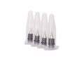
Conductive Ink
- Use to lay conductive traces on substrates (Green is "V1 Ink" setting on Reflow Oven)

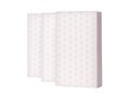
Solder Paste
- Use only on boards that utilize Voltera's ink traces, such as the ink above. (Orange is "V1 Paste" setting on Reflow Oven)

Solder Paste Sn63 Pb37
- Use only premade boards, such as ones from JLCPCB (Blue is "Sn63Pb37" on Reflow Oven)
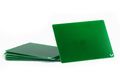
Substrates
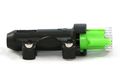
Probe
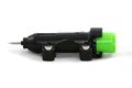
Dispenser and Sheath
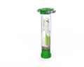
Conductive Ink Cartridge
Nozzle - 225 Micron
Burnishing Pads


Before you Print
Here are a few things to check before exporting your gerber files and fabricating your PCB.

- Verify via hole sizes.
- Based on the size of what needs to go in the via, select a rivet with the proper internal diameter from the table on the Through Hole Press page.
- Once you've selected the rivet size, take the outer diameter of the rivet from the table and add 0.1mm.
- Check this outer diameter against the available drill sizes for the Voltera (see the image to the right). Round up to the nearest drill size and use that for the hole size in Altium.
- Verify annular ring size
- Your annular rings (via diameter) should be at least as large as the head diameter of the rivets you plan to use, otherwise they might not make good contact.
- Check that your design follows the circuit design guidelines at the link above
Training
Operation
The PCB Printer is a fantastic tool for prototyping PCBs. After uploading Gerber files from Altium or a related software, the Voltera will be able to print traces and pads. The Voltera has the ability to bake traces and reflow components on its heated bed, but you will need to use the reflow oven to bake boards. The PCB Lab uses the reflow oven for baking due to the amount of people it needs to accommodate, so users will only be using the PCB Printer to print traces and pads. The Conductive Ink (used for Traces) is indicated by a green dot on the dispenser, the Voltera Solder Paste (used for Pads) is indicated by an orange dot on the dispenser, and the Manufactured Solder Paste (used for Pads) is indicated by a blue dot on the dispenser.
Before beginning with your PCB, it is imperative that it is completely flat, meaning no components are installed, as it will result in breaking the nozzle of the dispenser, or it will be unable to calibrate correctly.
Demonstration
To show a complete knowledge of the PCB Printer, the student will design a PCB in Altium or related software, print the traces/pads, and transition to the Reflow Oven. As a part of the process, the student will also perform correct set up and shut down procedures, all of which can be found in the General Procedure below.
General Procedure
Using the Voltera to create single-sided boards with NO vias or holes.

- Drilling
- This board in particular does not have any holes, so this entire step can be skipped for this procedure, however, these are the steps to take if you need to drill holes in the future.
- After opening the Voltera software, select Drill. This option is chosen only if you want to add holes to an existing board.
- For Drilling, you can either choose the Simple or Aligned route. Choose Simple if your board has no existing features, and choose Aligned if your board has some existing features. Lets go through the process for both.
- Drilling for a Simple Board
- Alrighty, you've chosen Simple, so this procedure assumes there is absolutely nothing fabricated on the board. Not gonna lie, this procedure is a little more sketchy than aligned simply because you literally eyeball your board's outline. The no eloquent calibration system. That's just how it works.
- Voltera will ask you to upload your Ink and Hole files. Remember, the correct Hole file will say Plated in the name. This will allow you to calibrate the Voltera later and it supplies the drill locations.
- Then it will ask you to move your boards location on the plate so the Voltera knows where it needs to drill. This is the sketchy part. It outlines a square, and you make a judgement based on what it thinks. If it outlines too low, move your circuit up further on the plate to compensate for it. If it outlines too far to the left, move your circuit to the right on the plate to compensate for it. Continue this process until it looks "good enough."
- Use the clamps and screws to secure your board. It would be such a shame if it moved during fabrication...
- Mount the probe on machine. This will help us calibrate the machine. It will move to the wrong spot initially, but then it is your duty to move the probe into the correct spot. Lowering the probe will allow you to make fine tune movements to optimize the alignment.
- Once the alignment is complete, it will measure the height of every part of the board. It will take a couple minutes, so just be patient. The transition between printing and drilling is done with the same alignment.
- Once that is complete, it is time to select the holes we want to drill. All the holes you select are highlighted in Green. Remove the probe and select which holes you want to drill. Remember not to drill the holes that already exist!
- Select the corresponding drill bit, put it into the drill, mount it, and plug it in. Be extra careful not to break anything. People usually break it because while they are mounting it, the drill hits the Voltera and snaps. It's okay to push it into the drill pretty far, and this will keep you from breaking it. DON'T FORGET TO USE THE ALLEN WRENCH TO SECURE THE BIT!
- The drill should sing you a little song once it's connected. Before drilling, prepare the vacuum. Use this to suck all the debris that comes from your board. You can get it decently close to the board, even on the board while it is drilling, just be sure to move when the drill is getting ready to move.
- And you're finished drilling holes! Vacuum up any debris and continue with laying the traces.
- Drilling for an Aligned Board
- Awesome, you've chosen Aligned, so this procedure assumes you have some preexisting holes and the like on the board.
- Voltera will ask you to upload your Ink and Hole files. Remember, the correct Hole file will say Plated in the name. This will allow you to calibrate the Voltera later and it supplies the drill locations.
- Use the clamps and screws to secure your board. It would be such a shame if it moved during fabrication...
- Mount the probe on machine. This will help us calibrate the machine. It will move to the wrong spot initially, but then it is your duty to move the probe into the correct spot. Lowering the probe will allow you to make fine tune movements to optimize the alignment.
- Once the alignment is complete, it will measure the height of every part of the board. It will take a couple minutes, so just be patient.
- Once that is complete, it is time to select the holes we want to drill. All the holes you select are highlighted in Green. Anything that is highlighted in Green will be executed. Remove the probe and select which holes you want to drill. Remember not to drill the holes that already exist!
- Select the corresponding drill bit, put it into the drill, mount it, and plug it in. Be extra careful not to break anything. People usually break it because while they are mounting it, the drill hits the Voltera and snaps. It's okay to push it into the drill pretty far, and this will keep you from breaking it. DON'T FORGET TO USE THE ALLEN WRENCH TO SECURE THE BIT!
- The drill should sing you a little song once it's connected. Before drilling, prepare the vacuum. Use this to suck all the debris that comes from your board. You can get it decently close to the board, even on the board while it is drilling, just be sure to move when the drill is getting ready to move.
- And you're finished drilling holes! Vacuum up any debris and continue with laying the traces.
- Ready the Ink
- The ink is most usable when it reaches room temperature, so we have to let it warm up in advance.
- Grab the correct conductive ink from the fridge, and let it warm up to room temperature, about 15-30 minutes. It is labeled with a green sticker.
- Software Setup
- Download the files for this project here.
- Power on the Voltera.
- Open the Voltera Windows application.
- Select "Print" and then "Simple." "Print" indicates that we want to print traces, and "Simple" indicates that the board is not pre-fabricated. If we had a pre-fabricated board, we would instead select "Aligned" so we can align the holes.
- Next we need to add the proper conductive ink, which is the same conductive ink you acquired in step 1.2.
- Load the ink file from the project files. This is the Top Layer Gerber file.
- Clamping the Substrate
- Acquire a 1.5" by 2" blank board. They are located in the one of the drawers.
- Slide the board underneath the clamps on the Voltera, push the clamps towards each other, and finger-tighten the thumb screws. You should not be able to move the board once you clamp them down.
- Mounting the Probe
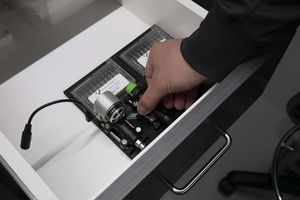
- Pull the probe from one of the drawers. The probe should have a large metal tip, do not confuse it with the dispenser.
- Remove the cap and place it near the Voltera.
- Mount the probe onto the magnetic gantry. It should snap into place and the contacts should align.
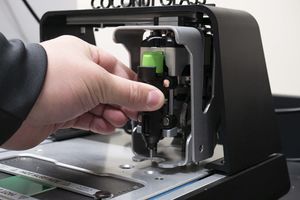
- Pull the probe from one of the drawers. The probe should have a large metal tip, do not confuse it with the dispenser.
- Positioning and Probing
- Click "Outline." This will show you where the Voltera thinks the board is. It will move the probe around the printer surface and determine how close the dispenser will need to be to the board.
- Repeat step one until the outline is centered with the board. Click and drag the circuit in the Voltera application to move the outline.
- You MUST ensure the outline does not collide with the clamps AND does not exceed the dimensions of the board! Do NOT proceed until this is checked!
- In the next step, Click "Probe" and wait for the Voltera to finish its measurements.
- Remove the probe, replace the cap, place the probe back in the drawer, and proceed.
- Priming the Conductor
- Ensure 15 minutes have passed before beginning the next step. This helps the ink flow easier, so the dispenser should not be cold to the touch.
- Read carefully. The Voltera application explains this step well. Follow the on-screen instructions before moving on to the next step. Some tips/tricks/warnings:
- Nozzles are fragile! You would be surprised how easy it is to break one. Treat this process with care!
- Hold the dispenser over a paper towel to prevent ink from getting everywhere.
- If you need to wipe the nozzle, do so gently and use a cotton swab found in the drawers.
- Ink should not be flowing quickly out of the dispenser when you finish priming, but a very small amount of flow is OK.
- Mount the dispenser.
- Calibration
- Click "Advanced." Start with the Z at 0.10 mm and the E at 0 um. Adjust the Voltera to these values, as it is a safe distance for the dispenser.
- Click "Calibrate." The Voltera will lay down a test print. Pay close attention to the amount and consistency of the ink.
- The example below has slightly too much ink. Notice how a portion of the horizontal lines touch and some parts of the ink glob up.
- In this case, to make an adjustment, the ink height was set to a Z of 0.09 mm and the flow was set to an E of -10 um. This dispenses less ink than before.
- You may need to do the same or make different adjustments. Whatever you do, do NOT run the nozzle into the board! The nozzle will break!
- If an adjustment was made, wipe the board clean with a paper towel (shown below) and/or clean it with isopropyl alcohol and repeat the calibration.
- The example below is a more acceptable test print. Strive for this consistency. If your board looks right, proceed.
- Click "Next," and wipe the board clean a final time, as you are now preparing to print your whole circuit.
- Top Layer Print
- The Voltera will print what is selected in Green. Below is an example of a portion of the board selected. Ensure the portion you want to print is selected (in this case, select everything.) Remember that blue lines will not be printed.
- Click "Start." Let the Voltera finish its process. If a portion of the print fails or is incorrect, you can stop mid-print, or wait until it is finished and redo that selection. Also shown below is an example of a portion of ink that globbed up. The portion was wiped and can be reprinted.
- Remove the conductive ink, put the cap back on, and return the conductive ink to the fridge!
- When you reach the instruction titled "Flip Board," you are done. We want to bake these traces on the Reflow Oven before we do anything else to the board.
- Unclamp the board from the Voltera, and remember that the traces are still wet, so do not smear them around.
- Consult the Reflow Oven wiki and complete that process. Bake the board soon after printing to ensure best results.
- The Voltera will print what is selected in Green. Below is an example of a portion of the board selected. Ensure the portion you want to print is selected (in this case, select everything.) Remember that blue lines will not be printed.
- Preparing for Solder Paste
- You should now have a PCB with traces baked on it! Time to make those pads for placing components.
- Take a burnishing pad from one of the drawers. Rub the substrate with the pad until the traces have a shine to them, rather than a dull appearance.
- Replace the burnishing pad back into the drawer. This cleans the surface of the traces and makes them look super shiny.
- Aligning the Paste
- This process will help the Voltera know where it needs to print solder. The user gives it two locations where the pads should go, and the Voltera can use the Gerber files to determine where else pads need to go.
- At this time, retrieve the solder paste from the fridge and set it out to warm. The correct paste is labeled with an orange sticker.
- Take the board back to the Voltera and clamp the board into place. Again, you should not be able to move the board after it is clamped.
- Open the Voltera application and choose "Solder," and choose the proper paste. In this case you want the orange-labeled paste.
- Clean the calibration switches, mount the probe, and proceed.
- Click 'Move to feature." This will move the probe to a pre-determined feature and should not be aligned properly on the first go. It is your job to align it correctly.
- First, use the arrow keys to roughly align the feature with the probe. This process will help the Voltera know where it needs to put the pads.
- Next, click "Lower," and use the arrow keys to fine-tune the alignment. Your precision in these steps is key to getting solder paste in the correct places.
- Click "Measure" when the alignment is correct. The board will be probed and the head will move to a second feature.
- Repeat steps 8 and 9.
- Click "Measure." The alignment is now finished.
- You can confirm the alignment by clicking various features and seeing if the head moves to the right position. If something is off, you can go back and realign if necessary. Proceed until you need to measure the height of the board.
- Click "Probe." This will measure the height of the board and determine how far away the dispenser needs to be from the board.
- Once it finishes probing, remove the probe and replace it in the drawer.
- Priming the Paste
- Refer to the priming directions in step 8 before mounting the dispenser.
- Once it is primed, mount it and proceed.
- Click "Dispense." The paste will dispense onto all of the selected pads.
- Strive for good coverage of paste, preferably covering most of the pad, if not all of it.
- Remove the dispenser. Twist the knob clockwise to back off the paste. Put it back in the fridge, and quit the Voltera app.
- Unclamp the board from the Voltera. Remember that you are handling a board with wet paste. Clean up!
- Cleaning up
- Clean any leftover paste or ink from the calibration switches by rubbing them with a dry cue tip before it dries.
- If any ink or paste remains elsewhere on the machine, use a cue tip or kimwipe with a little bit of isopropyl alcohol to clean it. Be careful not to drench the machine in isopropyl, as it could let gunk get into the machine and jam things up.


You are now done with the PCB Printer! Refer to the Pick and Place as well as the Reflow Oven wikis for the remainder of the process.
Safety
- When the PCB Printer is moving and doing its thing, just let it be. Interfering will result in breaking equipment and possibly hurting yourself, especially with the drill. Voltera gives excellent advice/steps for their PCB fabrication process, be sure to follow them.
- If you feel like you do not know what you are doing, ask someone for help. You could damage both the equipment and possibly hurt yourself. Do not hesitate to ask or confirm at any point during the process.
Certification
Troubleshooting
- Drilling
- If your holes seem to be all out of wack, be sure to confirm the following: you should be using the vacuum to suck up any debris that comes from drilling your board while it is drilling. The pieces can interfere with your part.
- If they seem to be drilling in the wrong places, then it probably isn't aligned correctly. Go back in the process and start over.
- Calibration/Alignment
- During the probing process, be sure that your board is completely flat and that the clamps cover a minimal amount of the board while keeping it secure. If the probing hits the claps or runs off the board, the calibration is no good. Go back to the initial stages where you align holes/indicate where to print traces.
- When holes are available during the Alignment stage, always use them to align your board. NEVER use pads or traces unless you absolutely have to. Holes are much easier to align with.
- Printing Traces/Solder
- Be sure that the dispenser has been warming up to room temperature for at least 15 minutes so the ink can flow smoothly.
- If the ink does not seem come come out even when you're priming the dispenser, chances are that it is clogged. Remove the tip, notify a PCB Lab worker, and install a new tip (ask a worker if you don't know how).
Maintenance
General maintenance
The PCB Printer has a few items that need to be maintained by the student or the Ace. Refer to the table below to see each procedure, how often it should occur, and the the last completion of the specific task.
Specific Maintenance Tasks
| Maintenance Procedure | Frequency | Done By | Last Completion |
|---|---|---|---|
| General Cleaning | Before and after each use, including ink/solder residue and drilled material | Student | N/A |
| Refrigerating the Dispensers | Whenever they are not in use | Student | N/A |
| Replacing Sacrificial Layer | When the existing layer is worn through and can potential damage the heating bed | Ace | |
| Replacing Nozzle | When the nozzle is clogged | Student or Ace | |
| Replacing ink/solder paste syringe | Whenever out of ink/solder paste | Ace | 01/27/2022 by MM |
| Labeling dispenser with lot name | Whenever ink/solder paste is replaced | Ace | 01/27/2022 by MM |
| Cleaning calibration switch linear hardware (Disassemble, clean, oil) | Once yearly, or as required. | Ace and Technician | 01/27/2022 by MM |